-
×InformationNeed Windows 11 help?Check documents on compatibility, FAQs, upgrade information and available fixes.
Windows 11 Support Center. -
-
×InformationNeed Windows 11 help?Check documents on compatibility, FAQs, upgrade information and available fixes.
Windows 11 Support Center. -
- HP Community
- Desktops
- Desktop Boot and Lockup
- Re: Jumper diagram incorrect for clearing CMOS/BIOS/RTC/Pass...

Create an account on the HP Community to personalize your profile and ask a question
04-19-2018 05:40 PM - edited 04-19-2018 07:28 PM
Hello,
I am looking for an accurate diagram and function of the jumper settings for the:
- ROM_RECOVERY
- CMOS+PW
- FLASH_OVERRIDE (labelled as "FDO" on the motherboard)
for an HP Envy H1420t, motherboard =
- Manufacturer name: Pegatron
- Motherboard name: IPMMB-FM
- HP/Compaq name: Formosa
- SSID: 2AD5h
I have not been able to reset the BIOS/CMOS because I cannot determine which jumper settings are for reset.
The support page on the HP website has diagrams with PIN locations for ROM_RECOVERY and CMOS+PW pins, but nothing about the FLASH_OVERRIDE pins.
Additionally, the HP support page diagrams are incorrect. They have a different number of pins and jumper setups than are on the actual motherboard.
I would appreciate any help in determining:
1. Which jumper settings correspond to which numbers on the pins?
e.g. if instructions say to move jumper from 1-2 to 2-3, how can someone know which pin is "1" and which is "3"? The (incorrect) diagrams on the HP support website assume that the viewer is looking at the pins from a specific, unknown rotation.
2. What are the actual reset and "normal" jumper settings for the ROM_RECOVERY and CMOS+PW for this motherboard?
The diagrams in the HP support page apply to a different set of pins.
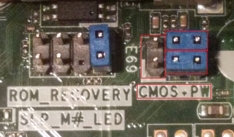
- There are 2 sets of jumpers (not 1) on the CMOS+PW pins
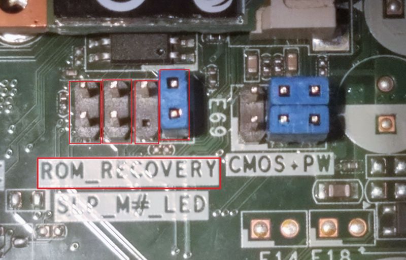
- There are 7 pins (not 6) on the ROM_RECOVERY.
- The default jumpers are not at all like the ones depicted in the support page.
3. What is the function of the FLASH_OVERRIDE ("FDO") pins?
Below is a comparison of the HP support for this motherboard versus pictures of the actual motherboard (with the jumpers on their default settings).
ROM_RECOVERY
- HP Support:
- Actual Motherboard (note that there is a pin missing next to the jumper on the bottom)
CMOS+PW
- HP Support:
- Actual Motherboard
Thank you!
Solved! Go to Solution.
Accepted Solutions
09-03-2019 10:18 AM
I think you may have made one incorrect assumption:
In the first photo, you're associating "ROM_RECOVERY" with HP Support "CMOS" jumper pins. I think that's wrong. I believe both HP Support diagrams are referring ONLY to the CMOS+PW jumpers (2 rows of 3 pins, 6 total).
So: "CMOS" refers to pins 2,4,6 (first row)
and: "PW": refers to pins 1,3,5 (second row)
and nothing in the HP Support info refers to "ROM RECOVERY".
Maybe one piece of information might help in identifying Pin 1 on any printed circuit board: PIN 1 is usually indicated by a heavy (thicker) printed (usually white) line.
Looking at your photos, there is a white thin line around CMOS+PW jumpers. You'll notice one corner of the rectangle has a thicker line to it in the bottom left of your photo. That would seem to indicate that your motherboard is rotated 90deg to the right of their schematic's orientation.
They are stupidly showing a schematic that ignores the jumper on 4-6, row 1, when they are referring to the jumper on 3-5 , row 2, and vice versa.
For ROM RECOVERY, I would just move the jumper around to different positions and hope you hit the right combination. If your PC isn't booting anyway, it can't hurt.
04-19-2018 09:18 PM - edited 04-19-2018 09:34 PM
Hi,
HP doesn't disclose the information and documentation for doing ROM recoveries. That information is held close to the chest.
I agree with you about the Clear CMOS and Clear password jumper settings. The posted information doesn't reflect the jumpers on the actual Formosa motherboard. Moving the jumper over to cover the vacant pin using the written instructions should get the job done.
You can always reset the CMOS by removing the CMOS battery for 60 seconds. Unplug the PC, hold down the power button for 60 seconds and now remove the CMOS battery for 60 seconds should get the job done.
I'll let HP know about the documentation discrepancy.
----------------------------
The Formosa motherboard was also used in the Pavilion series. Hopefully this is not the tip of the iceberg with other motherboards.
09-03-2019 10:18 AM
I think you may have made one incorrect assumption:
In the first photo, you're associating "ROM_RECOVERY" with HP Support "CMOS" jumper pins. I think that's wrong. I believe both HP Support diagrams are referring ONLY to the CMOS+PW jumpers (2 rows of 3 pins, 6 total).
So: "CMOS" refers to pins 2,4,6 (first row)
and: "PW": refers to pins 1,3,5 (second row)
and nothing in the HP Support info refers to "ROM RECOVERY".
Maybe one piece of information might help in identifying Pin 1 on any printed circuit board: PIN 1 is usually indicated by a heavy (thicker) printed (usually white) line.
Looking at your photos, there is a white thin line around CMOS+PW jumpers. You'll notice one corner of the rectangle has a thicker line to it in the bottom left of your photo. That would seem to indicate that your motherboard is rotated 90deg to the right of their schematic's orientation.
They are stupidly showing a schematic that ignores the jumper on 4-6, row 1, when they are referring to the jumper on 3-5 , row 2, and vice versa.
For ROM RECOVERY, I would just move the jumper around to different positions and hope you hit the right combination. If your PC isn't booting anyway, it can't hurt.
![c03246643[1].jpg c03246643[1].jpg](/t5/image/serverpage/image-id/180242i90B602AF6C9D29CB/image-size/large?v=v2&px=999)

![c03246644[1].jpg c03246644[1].jpg](/t5/image/serverpage/image-id/180244iAFA69A0068EFF9D7/image-size/large?v=v2&px=999)

